Shopping Cart


TRAINING & EDUCATION SYSTEMS
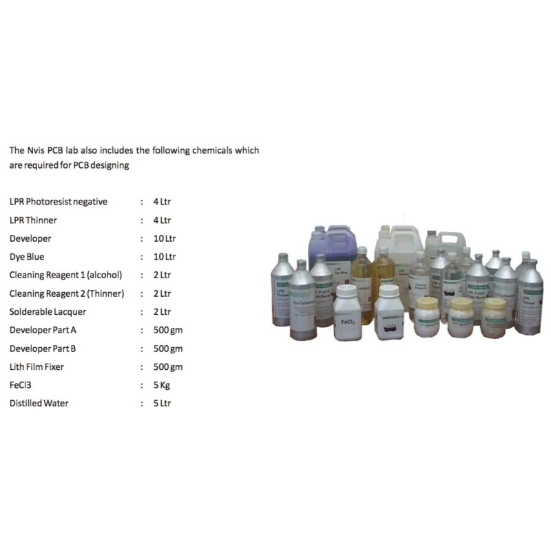
Nvis PCB LAB is a complete solution for designing PCB. This solution includes all the necessary machines and chemicals which are used in the PCB development process.
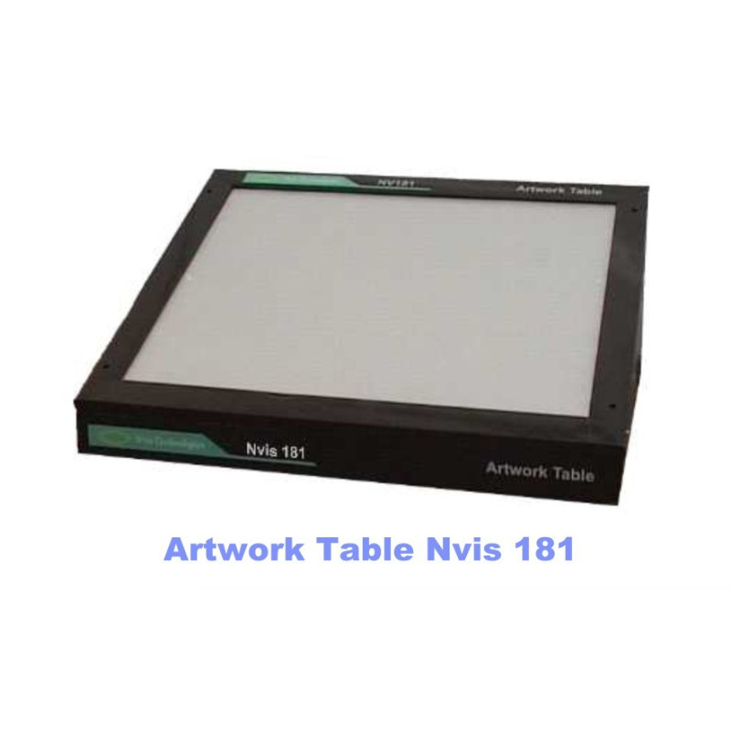
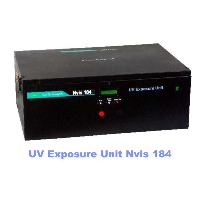
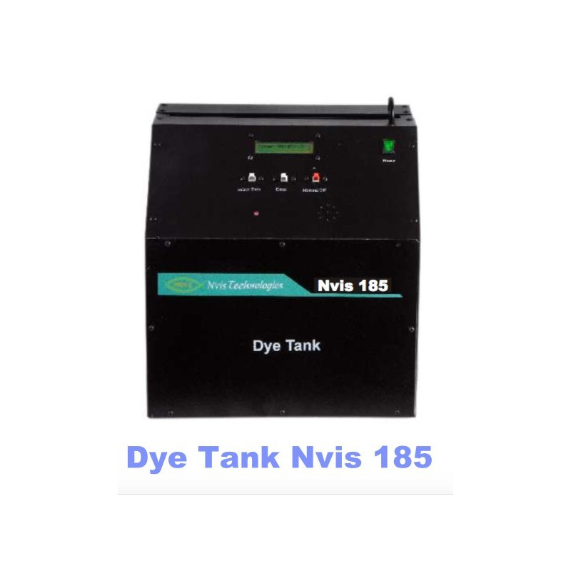
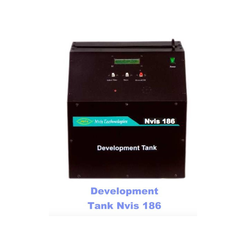
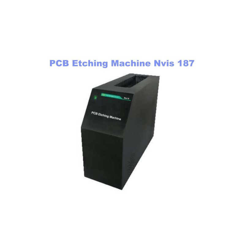
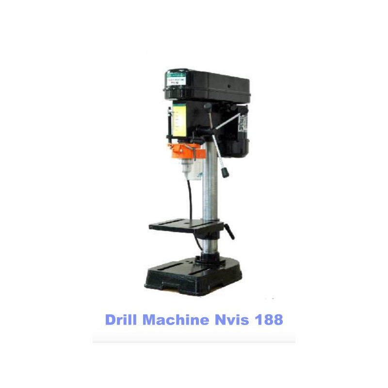
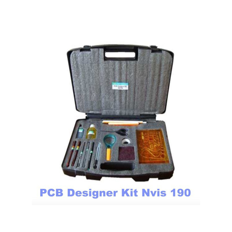
The PCB artwork film maker is used as a contact printer for creating design films from the PCB Layout. The artwork table is used for manually designing the films and for correcting or changing the existing films. The shearing machine is used for cutting the PCB according to film size. The photoresist dip coating machine is used for coating photoresist on the PCB Laminate. After photoresist coating, the PCB and films are placed in UV exposure machine for exposing. After exposing the development tank is used to remove unused photoresist. The dye tank is used for highlighting the design on the PCB. The etching machine is used for removing unused copper from the PCB. The drilling machine is used for making the holes in the PCB. The PCB design kit is provided which include tapes, stencils and other accessories used for designing the PCB.


